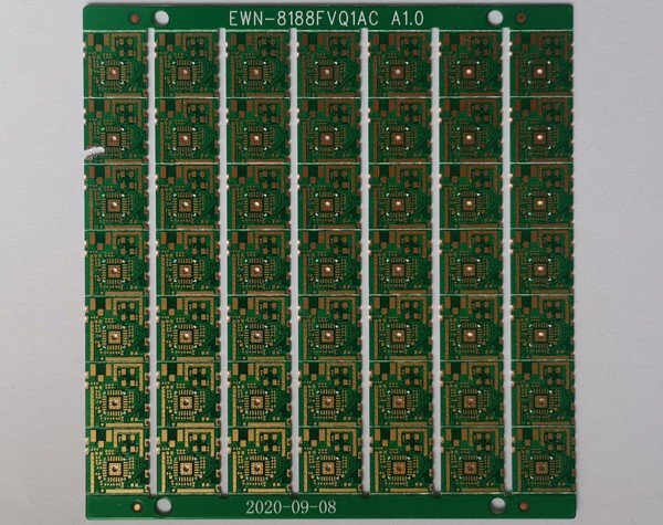


1. Cutting
Intent: According to the requirements of the engineering data MI, on the large sheets that meet the requirements, cut into small pieces of production boards, which meet the small pieces of customers required by the customer.
Process: large sheet → cutting board according to MI requirements → curium board → beer fillet edging → ejecting board
2. Drilling
Intent: According to the engineering data, drill the required hole diameter at the corresponding position on the sheet material that meets the required size.
Process: stacked board pin → upper board → drilling → lower board → view repair
3. Immersion copper
Intent: Copper sinking is to use chemical methods to deposit a thin layer of copper on the wall of the insulating hole.
Process: rough grinding → hanging board → automatic copper sinking line → lower board → dip% dilute H2SO4 → thickened copper
4. Graphic handling
Intent: Graphic transfer is to transfer the pictures on the production film to the board
Process: (blue oil process): grinding plate → printing one side → drying → printing two sides → drying → exploding → developing shadow → viewing; (dry film process): hemp board → lamination → standing → alignment → exposure →Set aside→Print the shadow→View
5. Graphic plating
Intent: Pattern electroplating is to electroplate a copper layer with a required thickness and a gold-nickel or tin layer with the required thickness on the exposed copper skin or hole wall of the circuit pattern.
Process: upper board → degreasing → twice water washing → micro-etching → water washing → pickling → copper plating → water washing → pickling → tin plating → water washing → lower board
6. Removal of the film
Intent: Use NaOH solution to remove the anti-plating coating film to expose the non-circuit copper layer.
Process: water film: inserting rack → soaking alkali → flushing → wiping → passing machine; dry film: putting board → passing machine
7. Etching
Intent: Etching is to use a chemical reaction method to corrode the copper layer of non-circuit parts.
8. Green oil
Intent: Green oil is to transfer the graphics of the green oil film to the board to maintain the circuit and prevent the tin on the circuit when welding parts
Process: grinding plate → printing photosensitive green oil → curium plate → exposure → developing shadow; grinding plate → printing one side → drying plate → printing two sides → drying plate
9. Characters
Intent: Characters are provided as a mark for easy identification
Process: After the green oil finishes → cool and stand → adjust the screen → print characters → rear curium
10.Gold-plated fingers
Intent: Plating a layer of nickel and gold with the required thickness on the fingers of the plug to make it more hard and wear-resistant
Process: upper plate → degreasing → washing twice → micro-etching → washing twice → pickling → copper plating → washing → nickel plating → washing → gold plating
Tin plate (a process in parallel)
Intent: Tin spraying is to spray a layer of lead tin on the exposed copper surface that is not covered with solder mask to protect the copper surface from corrosion and oxidation to ensure good soldering performance.
Process: micro-erosion → air drying → preheating → rosin coating → solder coating → hot air leveling → air cooling → washing and air drying
11. Forming
Intent: through die stamping or CNC gong machine gongs to produce the shape required by the customer. Organic gongs, beer board, hand gongs, hand-cut
Note: The accuracy of the data gong machine board and the beer board is high. The hand gong is second, and the hand-cutting board can only make some simple shapes.
12. Quiz
Intent: After an electronic 100% test, detect open circuits, short circuits and other shortcomings that affect functionality that are not easy to find visually.
Process: upper mold → release board → test → pass → FQC visual inspection → unqualified → repair → return test → OK → REJ → scrap
The above is the circuit board process flow? An introduction to the pcb circuit board production process. If you want to know more information about pcb circuit boards, you can pay attention to Jingchuangda circuit board manufacturer.
(Some materials on this website come from the Internet. If the information displayed on this website infringes your copyright or other legal rights, please notify us in time, and this website will be deleted in time.)
Call
0750-8525120

Scan